Semiconductor and IC Packaging Materials Market Size, Trends, Segments, Share and Companies 2025-35
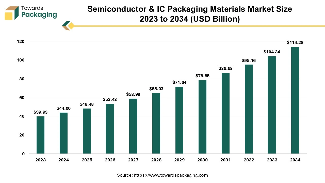
According to projections from Towards Packaging, the global semiconductor and IC packaging materials market is set to increase from USD 53.48 billion in 2026 to nearly USD 114.28 billion by 2034, reflecting a CAGR of 10.2% during 2025 to 2034.
Ottawa, Nov. 26, 2025 (GLOBE NEWSWIRE) -- The global semiconductor and IC packaging materials market generated revenue of USD 48.48 billion in 2025, and this figure is projected to grow to USD 114.28 billion in 2034, according to research conducted by Towards Packaging, a sister firm of Precedence Research.
The significance of the semiconductor and IC Packaging Materials market depends on its vital role in enabling modern electronics by protecting, connecting, and managing the performance of integrated circuits (ICs).
Request Research Report Built Around Your Goals: sales@towardspackaging.com
What is Meant by Semiconductor and IC Packaging Materials?
Semiconductors are materials such as silicon that have electrical conductivity between that of a conductor and an insulator. IC (Integrated Circuit) packaging is the procedure of encasing a semiconductor chip in a protective casing to then shield it from environmental damage, facilitate its connection to few circuits, and dissipate heat. This market is significant because packaging materials are important for the functionality, reliability, and even miniaturization of devices, which are driven by the expansion of consumer electronics, automotive, and with telecommunications sectors.
The main drivers for the semiconductor and IC packaging materials market are the rising demand for consumer electronics and even advanced technologies such as 5G, AI, and IoT. These technologies need more sophisticated, smaller, and thus, higher-performing semiconductor devices, which in turn drives the requirement for advanced packaging materials that can enhance thermal performance, electrical properties, as well as miniaturization.
Key Government Initiatives for the Semiconductor and IC Packaging Materials Industry:
- U.S. CHIPS and Science Act: The United States allocated over $52.7 billion in federal subsidies and tax credits to incentivize domestic semiconductor manufacturing, research, and development to reduce reliance on foreign supply chains.
- EU Chips Act: This European Union regulation seeks to mobilize €43 billion in public and private investments to double its global market share to 20% by 2030, focusing on research, innovation, and establishing "first-of-a-kind" production facilities.
- China's Big Fund (National Integrated Circuit Industry Investment Fund): China established this state-backed investment fund to provide substantial financial support to its domestic semiconductor industry, aiming for technological self-sufficiency and reducing dependence on imports.
- Japan's Semiconductor Strategy (Rapidus initiative): Japan is leveraging government-backed funds and strong international collaboration (e.g., with IBM and imec) to establish cutting-edge logic chip manufacturing capabilities through the new foundry Rapidus.
-
India Semiconductor Mission (ISM): India offers significant fiscal support and incentives, including a Design Linked Incentive (DLI) scheme and capital expenditure subsidies, to foster a comprehensive domestic ecosystem for chip design, manufacturing, and advanced packaging (ATMP/OSAT).
Get All the Details in Our Solutions - Access Report Sample: https://www.towardspackaging.com/download-sample/5258
What are the Latest Trends in the Semiconductor and IC Packaging Materials Market?
-
Adoption of Advanced Technologies
Due to the demand for higher performance, miniaturization, and reliability. Advanced packaging is important to create smaller, faster, and even more power-efficient chips, and to handle challenges such as thermal management and signal integrity that are vital for these new applications. The need for faster and more reliable wireless communication demands high-performance chips and innovative packaging solutions, such as antenna-in-package, to manage high frequencies and data volumes. The need for faster and more reliable wireless communication requires high-performance chips and also innovative packaging solutions, such as antenna-in-package, to manage high frequencies and data volumes.
-
Development of High-performance Materials for 5G and AI
5G needs ultrafast data processing and thus, minimal delay for applications such as autonomous vehicles, which is only possible with advanced packaging and materials that ensure optimal signal integrity. As chips become more powerful along densely packed, they generate more heat. High-performance materials are important for dissipating this heat, guaranteeing the reliability and even longevity of the devices. Technologies such as autonomous vehicles need semiconductor elements to perform reliably under demanding conditions. Advanced materials are key to ensuring the durability as well as performance of these components in harsh automotive environments.
What Potentiates the Growth of the Semiconductor and IC Packaging Materials Industry?
-
Increasing Demand for Smaller, More Powerful Electronic Devices
By necessitating advanced packaging solutions that enable miniaturization, improve performance, enhance thermal management, and guarantee reliability. This need pushes the acceptance of innovative packaging technologies and then specialized materials. Smaller devices usually rely on batteries, so power efficiency is vital. Advanced packaging solutions decrease power consumption via shorter electrical connections and even more efficient integration, which in turn drives the need for materials optimized for low power loss.
More Insights of Towards Packaging:
- Plastic Tray and Container Market Size, Trends, Segmentation, Regional Outlook and Competitive Landscape Report 2025-2035
- Recyclable Shrink Film Market Size, Trends, and Competitive Landscape: Global Industry Forecast to 2035
- Beer Glass Packaging Market Size, Share, Trends, and Forecast 2025-2035
- Dairy Aseptic Packaging Material Market Size, Trends, Segmentation, and Regional Outlook 2025-2035
- Duplex Paper for FMCG Market Size, Growth Trends, Segmentation, Regional Insights, and Competitive Landscape Forecast 2025-2035
- Plastic Turnover Box Market Size, Trends, Competitive Landscape, Global Industry Analysis, Segments, and Forecast 2025-2035
- Rigid Chilled Food Packaging Market Size, Share, and Forecast Analysis (2025-2035)
- Alcoholic Beverage Glass Packaging Market Size, Trends, Regional Insights (NA, EU, APAC, LA, MEA), Segments
- Canned Glass Packaging Market Size, Share, Trends, and Forecast 2025-2035
- Pillow Shape Aseptic Packaging Material Market Size, Share, Trends and Segment Forecast 2025-2035
- Beverage Closures Market Size, Share, Trends, Segments, and Regional Outlook to 2035
- Compostable Shrink Wrap Market Size, Share, Trends, Segments, Regional Outlook (NA, EU, APAC, LA, MEA), Manufacturers, Suppliers, and Competitive Analysis 2025-2035
- Daily Chemical Product Stand Up Pouches Market Size, Share, Trends, and Forecast Analysis (2025-2035)
- Retail Press Dispenser Pump Market Size, Share, Trends, Growth Forecast (2025-2035)
- Aseptic Processing and Packaging Market Size, Share, Trends, and Forecast Analysis (2025-2035)
- Fertilizer Bag Market Size, Trends, Segments, Regional Insights, and Competitive Landscape Report, 2025-2035
-
Bagging Machines Market Size, Trends, Share, Trends, Segments, and Regional Insights (NA, EU, APAC, LA, MEA)
Regional Analysis
Who is the Leader in the Semiconductor and IC Packaging Materials Market?
Asia Pacific leads the market because of a combination of factors, which include its status as a major production hub with advanced infrastructure, massive consumer electronics need, and strong government support. This ecosystem is reinforced by many deep supply chains, a high concentration of vast producers, and continuous government investment and innovation. Countries such as China, Taiwan, and South Korea leverage cost-efficient manufacturing and high-volume production, attracting global investment and now reinforcing their position as key growth areas.
China Semiconductor and IC Packaging Materials Market Trends
China's market is growing because of strong government support, high domestic need from consumer electronics and automotive sectors, and also advancements in domestic production capabilities. Key trends involve a push for self-sufficiency, expansion in high-performance packaging such as wafer-level packaging, the increasing usage of materials such as silicon carbide, and thus, an expanding domestic supply chain for materials along with equipment, despite continued reliance on imports for advanced chips.
India Market Trends
The Indian market for semiconductor and IC packaging materials is experiencing strong expansion, driven by government initiatives, a growing electronics sector, and an increasing need for advanced technologies such as 5G and AI. Key trends involve a shift towards domestic manufacturing, a target on miniaturization and even advanced packaging solutions, and a growing need for sustainable, eco-friendly materials.
How is the Opportunistic Rise of North America in the Semiconductor and IC Packaging Materials Industry?
North America's rise in the market is driven by remarkable government investment (e.g., the CHIPS Act), a strong focus on advanced packaging R&D, and high demand from key end-user industries such as AI, 5G, and automotive electronics. The U.S. CHIPS and Science Act offers billions in funding and incentives to drive domestic semiconductor production and advanced packaging capabilities, targeting supply chain resilience as well as reduced reliance on foreign suppliers. This has thus spurred significant private investments in the latest facilities, like Intel's expansion in Arizona and Amkor's recent advanced packaging facility location.
U.S. Semiconductor and IC Packaging Materials Market Trends
The U.S. market is undergoing robust growth driven by the need for advanced electronics in the consumer, automotive sectors, along with the 5G sectors. Key trends include the increasing demand for miniaturization, the acceptance of advanced packaging technologies such as wafer-level packaging, and a focus on developing innovative, high-performance, and also eco-friendly materials.
Canada Market Trends
Canada's market is undergoing strong growth, driven by global need and government funding for advanced manufacturing. Growth is boosted by booming sectors such as AI, automotive, along consumer electronics, all of which need high-performance, smaller, and thus, more efficient semiconductor devices.
Elevate your packaging strategy with Towards Packaging. Enhance efficiency and achieve superior results - schedule a call today: https://www.towardspackaging.com/schedule-meeting
Segment Outlook
Product Type Insights
Why did the Organic Substrate Segment dominate the Semiconductor and IC Packaging Materials Market in 2024?
This is because of its excellent balance of cost-effectiveness, performance, and even versatility. These materials, such as epoxy resins, are lightweight and thus, can be customized, permitting for the creation of small, high-density, along complex chips required for modern electronics. Their affordability as well as compatibility with high-volume production also led to their widespread use. Further, continuous development in organic substrate materials has enhanced their electrical and thermal performance, funding advanced applications and also fine-pitch interconnections for higher integration.
Packaging Technology Insights
Why did the Small Outline Package (SOP) Segment Dominate the Semiconductor and IC Packaging Materials Market in 2024?
This is due to its combination of low expense, compact size, and even compatibility with surface-mount technology (SMT). Its versatility for numerous lead counts and pin configurations, as well as efficient automated assembly processes, contributes to lower manufacturing expenses and faster production times. This makes it the ideal alternatives for a huge range of applications, mainly in the high-volume consumer electronics sector, where miniaturization is vital. They are programmed to be small and thin, enabling efficient usage of space on printed circuit boards (PCBs). This is important for compact and portable electronic devices such as smartphones, tablets, and wearables.
End-Use Insights
Why did the Consumer Electronics Segment dominate the Semiconductor and IC Packaging Materials Market in 2024?
This is due to the high need for devices such as smartphones, laptops, and even wearables, which need increasingly compact, high-performance, and even energy-efficient components. This demand drives the demand for advanced packaging techniques to production devices while integrating more functionality, which includes technologies such as 3D integration and fan-out wafer-level packaging. Devices demand to be power-efficient, mainly with the growth of wearables and then the demands of 5G technology, which creates a requirement for packaging that enhances both thermal management and electrical performance.
Recent Breakthroughs in the Global Semiconductor and IC Packaging Materials Industry
- In June 2024, Shin-Etsu Chemical developed a new instrument for manufacturing semiconductor package substrates utilizing a dual damascene method. This innovation eliminates the demand for interposers, reducing expenses and enabling microfabrication for developed semiconductor assembly.
Top Companies in the Semiconductor and IC Packaging Materials Market & Their Offerings
- LG Chem Ltd.: Supplies core packaging materials like dielectrics, laminates, and die attach films for advanced semiconductor integration.
- Jiangsu ChangJian Technology Co., Ltd. (JCET): Offers comprehensive outsourced semiconductor assembly and testing (OSAT) services for various ICs.
- Henkel AG & Co. KGaA: Provides a broad range of adhesive, encapsulation, and thermal management materials essential for chip packaging.
- Kyocera Corporation: Manufactures advanced ceramic and organic semiconductor packages (substrates) and related packaging materials.
- ASE: A global leader in outsourced semiconductor assembly and test (OSAT) services, providing full-service packaging solutions, including SiP.
- Siliconware Precision Industries Co., Ltd. (SPIL): Specializes in outsourced integrated circuit assembly and testing services as part of the ASE Group.
- Amkor Technology: Provides extensive contract microelectronics manufacturing, specializing in outsourced semiconductor packaging and testing services.
- Texas Instruments (TI): Designs and manufactures its own analog and embedded semiconductors, offering them in a wide variety of package types.
- IBIDEN CO., LTD.: A key supplier of high-performance, advanced plastic semiconductor packaging substrates, especially for high-end processors.
- Powertech Technology Inc. (PTI): Offers complete outsourced assembly and test (OSAT) solutions for memory and logic semiconductors, including bumping and probing.
Segments Covered in the Report
By Product Type
- Organic Substrate
- Bonding Wires
- Leadframes
- Encapsulation resins
- Ceramics packages
- Die attach materials
- Thermal interface materials
- Solder balls
- Others
By Packaging Technology
- Small outline package (SOP)
- Grid Array (GA)
- Quad flat no-leads (QFN)
- Dual Flat No-Leads (DFN)
- Quad flat packages (QFP)
- Dual-in-line (DIP)
- Others
By End-Use
- Consumer electronics
- Automotive
- Aerospace & Defence
- IT & telecommunication
- Healthcare
- Others
By Region
-
North America:
- U.S.
- Canada
- Mexico
- Rest of North America
-
South America:
- Brazil
- Argentina
- Rest of South America
-
Europe:
-
Western Europe
- Germany
- Italy
- France
- Netherlands
- Spain
- Portugal
- Belgium
- Ireland
- UK
- Iceland
- Switzerland
- Poland
- Rest of Western Europe
-
Western Europe
-
Eastern Europe
- Austria
- Russia & Belarus
- Türkiye
- Albania
- Rest of Eastern Europe
-
Asia Pacific:
- China
- Taiwan
- India
- Japan
- Australia and New Zealand,
- ASEAN Countries (Singapore, Malaysia)
- South Korea
- Rest of APAC
-
MEA:
- GCC Countries
- Saudi Arabia
- United Arab Emirates (UAE)
- Qatar
- Kuwait
- Oman
- Bahrain
- South Africa
- Egypt
- Rest of MEA
Invest in Our Premium Strategic Solution: https://www.towardspackaging.com/checkout/5258
Request Research Report Built Around Your Goals: sales@towardspackaging.com
About Us
Towards Packaging is a global consulting and market intelligence firm specializing in strategic research across key packaging segments including sustainable, flexible, smart, biodegradable, and recycled packaging. We empower businesses with actionable insights, trend analysis, and data-driven strategies. Our experienced consultants use advanced research methodologies to help companies of all sizes navigate market shifts, identify growth opportunities, and stay competitive in the global packaging industry.
Stay Connected with Towards Packaging:
- Find us on Social Platforms: LinkedIn | Twitter | Instagram | Threads
- Subscribe to Our Newsletter: Towards Sustainable Packaging
- Visit Towards Packaging for In-depth Market Insights: Towards Packaging
- Read Our Printed Chronicle: Packaging Web Wire
-
Get ahead of the trends – follow us for exclusive insights and industry updates:
Pinterest | Medium | Tumblr | Hashnode | Bloglovin | LinkedIn – Packaging Web Wire | Globbook | Substack | Bluesky | - Contact: APAC: +91 9356 9282 04 | Europe: +44 778 256 0738 | North America: +1 8044 4193 44
Our Trusted Data Partners
Precedence Research | Statifacts | Towards Healthcare | Towards Auto | Towards Food and Beverages | Towards Chemical and Materials | Towards Consumer Goods | Towards Dental | Towards EV Solutions | Nova One Advisor | Healthcare Webwire | Packaging Webwire | Automotive Webwire | Nutraceuticals Func Foods | Onco Quant | Sustainability Quant | Specialty Chemicals Analytics
Towards Packaging Releases Its Latest Insight - Check It Out:
- Box and Carton Overwrap Films Market Size, Trends, Key Segments, and Regional Dynamics with Manufacturers and Suppliers Data
- Airless Pumps Market Size, Trends, Key Segments, and Regional Dynamics with Manufacturers and Suppliers Data
- BioProcess Container (BPC) Market Size, Trends, Segments, Companies, Competitive Analysis, Value Chain & Trade Analysis 2025-2034
- 3D-Printed Stickers & Labels Market Size, Segments, Regional Data (NA/EU/APAC/LA/MEA) and Companies
- Aseptic Flex Bag Market Size, Trends, Segments, Companies, Competitive Analysis, Value Chain & Trade Analysis 2025-2034
- Compostable Packaging Labels Market Size, Trends & Forecast to 2035
- Biotechnology Labels and Packaging Market Size, Trends and Forecast Analysis by Product, Material, End-User, and Region (2025–2035)
- Reverse Tuck Box Market Size, Trends, Segments & Regional Forecast (2025-35)
- Automated E-Commerce Packaging Market Size, Trends & Forecasts (2025-2035) with Regional, Competitive & Trade Analysis
- IV Fluid Bags Market Size, Trends, Segments, Regional Insights & Competitive Landscape 2025-2035
- Plastic Tray Market Size, Trends, Segments, Regional Forecast (NA, EU, APAC, LA, MEA), Company Profiles & Value Chain Analysis
- Tablet Inspection and Printing System Market Size, Trends, Segments, Regional Insights & Supplier Landscape
- Duplex Paper and Board for FMCG Market Size, Trends, Segments, Regional Outlook & Competitive Landscape (2025-2035)
- Molded Tableware Products Market Size, Trends and Regional Insights (North America, Europe, APAC, Latin America, MEA)
- VCI Anti-corrosion Film Market Size, Trends, Competitive Analysis, Segments Data, Regional Insights, and Manufacturers
- Contact Lenses Packaging Market Size, Trends, Forecasts, Segment Analysis, Regional Insights, and Competitive Landscape
- Pharmaceutical Bottles Market Size, Trends, Segmentation, Regional Insights, and Competitive Landscape Analysis
- Veterinary Medicine Packaging Market Size, Trends and Segmental Analysis (2025-2035)

![]()
Legal Disclaimer:
EIN Presswire provides this news content "as is" without warranty of any kind. We do not accept any responsibility or liability for the accuracy, content, images, videos, licenses, completeness, legality, or reliability of the information contained in this article. If you have any complaints or copyright issues related to this article, kindly contact the author above.
